back to home▼


IoT Sensor |Micro Plasma|
Nano FET
| Organic TFT

Professor | Student |
Alumni
Notice | Lecture Journal | University

Nano FET

CMOSFET has been dramatically scaling down into nano ranges.
This aggressively device scaling causes significant short channel effect , poly depletion effect, band-to-band tunneling and increasing of gate direct tunneling. For these reasons, metal gate electrode , high-k dieletric material and SiGe strained channel are integrated current Nano Fet.
HMED studies 30 nm CMOS device design to maximize device performance using TCAD.
This study can provide guide line for CMOS processing integration when these processing technology are implemented in CMOS technology. [Electronic Lett, 2008 ], [EDL, 2008]

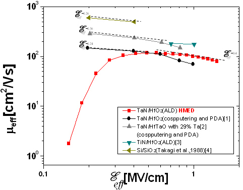
Fig 1. Measured mobility of Metal/high-k FET (20/30)

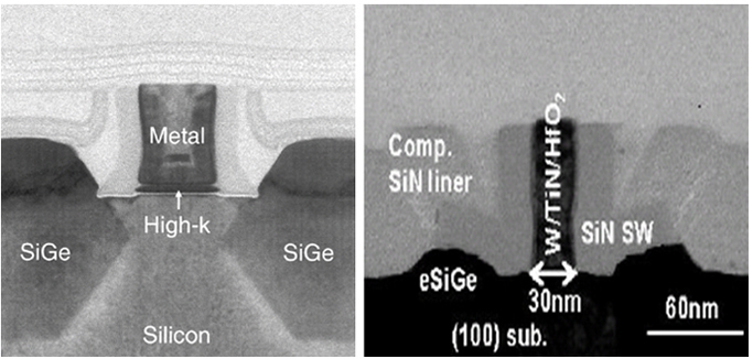
Fig 2. TEM micrograph of high-k + metal gate N/P MOS transistors (Intel, sony 2007)