|
|
|
|
|
|
| IoT Sensor | Micro Plasma | Ionic wind| Nano FET |
Professor | Student | Alumni |
Notice | Lecture | Journal | University | |
|
||||
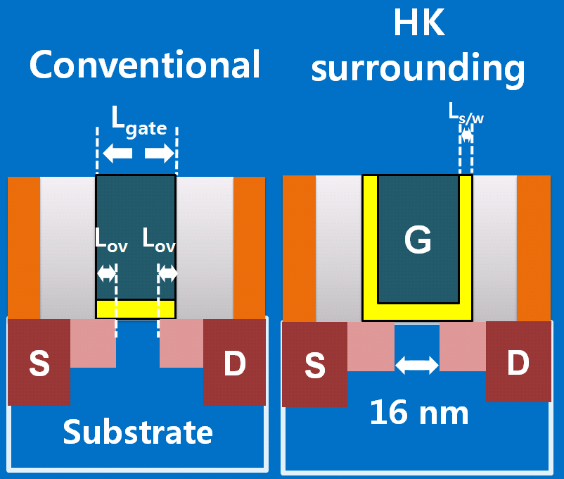
Nano FET Source/Drain Design for 16 nm Surrounding Gate MOSFETs A gate-last MOSFET has been suggested for 32 nm node CMOSFET, where the integration of a high-k gate dielectric and a metal gate electrode becomes essential to meet the transistor performance requirement. The gate-last MOSFET has been demonstrated as an effective integration scheme to avoid thermal instability and workfunction mismatch issues. We investigate an optimized S/D design for gate structures that had been reported for a 16 nm MOSFET. The high-k surrounding MOSFET is found to achieve comparable delay to the conventional gate structure, but the minimum delay is obtained with an underlap S/D, which is in contrary to the conventional one with an overlap S/D. It is also found that more underlap is preferred for the high-k surrounding gate MOSFET as the permittivity of the gate dielectric layer increases.
Fig.1 Designs of 16 nm CMOSFET
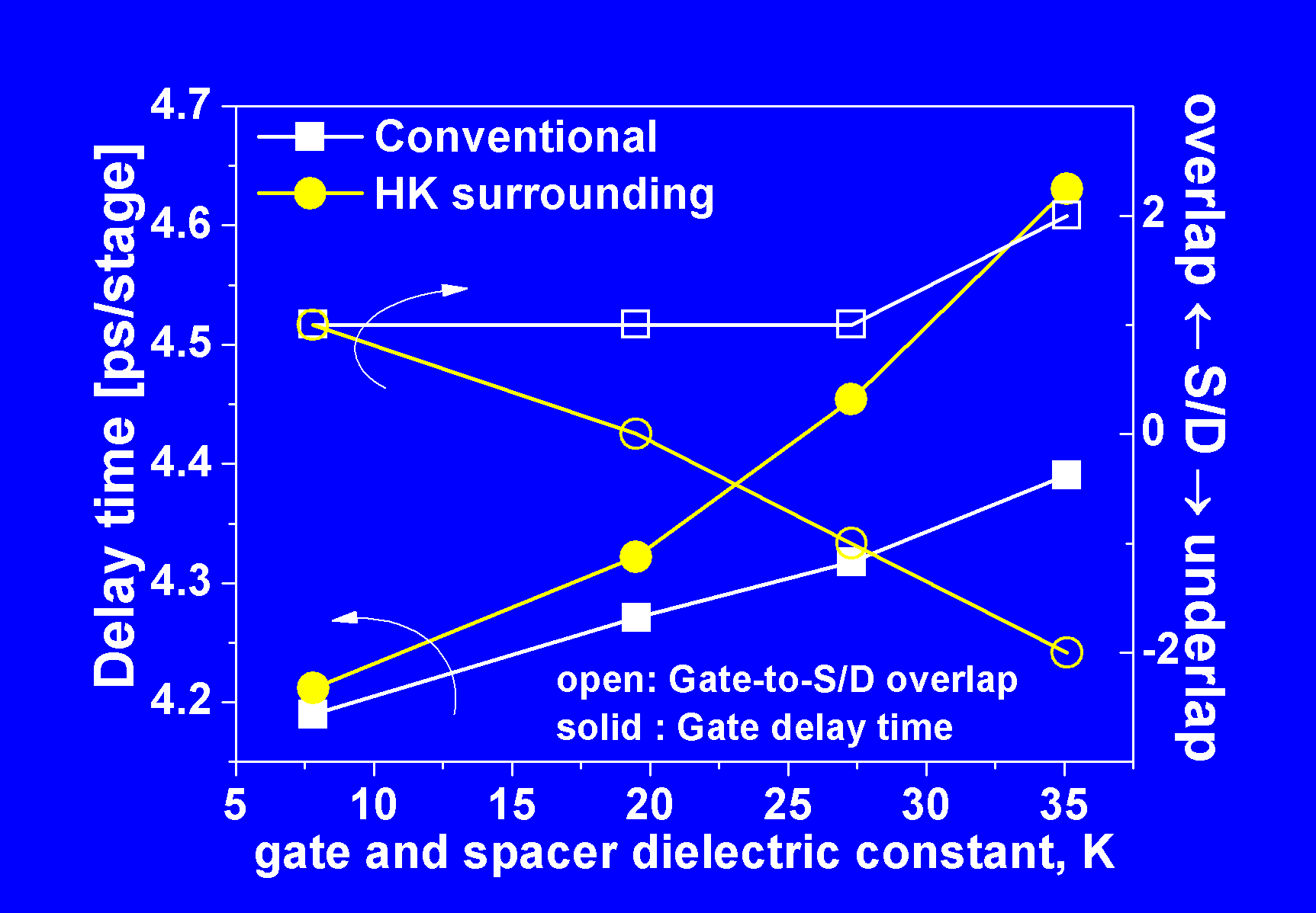
Fig. 2 Delay time and overlap length vs both gate and spacer dielectric constant for gate structures with optimized S/Ds. |
||||
CMOSFET has been recently scaling down into nano range and such aggressive scaling causes significant short channel effect, poly depletion and increasing gate tunneling. To overcome some of issues, metal/high-k gate stack and strained channel are integrated for nano FETs. HMED researches 30 nm CMOSFET design for maximizing device performance using TCAD and it will provide guidelines for CMOS process integration to realize optimized nano FET, such as gate stack and S/D overlap design (Electronic Lett[2008], IEEE EDL[2008]).
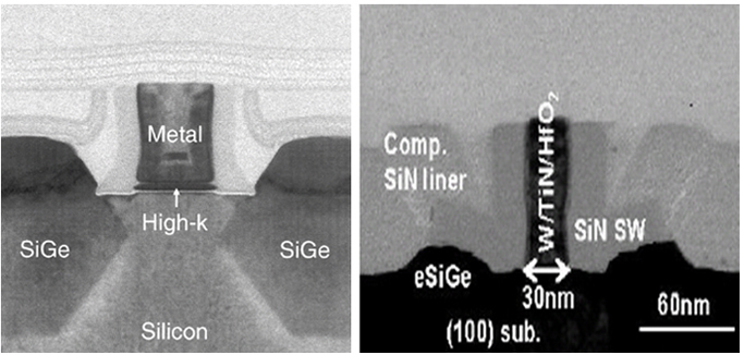
Fig 3. TEM micrograph of high-k + metal gate N/P MOS transistors (Intel, sony 2007)
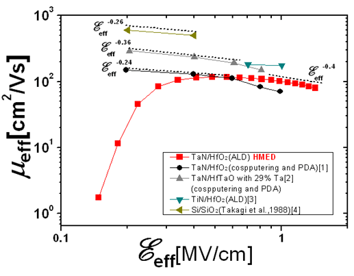
Fig 4. Measured mobility of Metal/high-k FET (20/30) |
||||
|
||||